
Applied Materials and BE Semiconductor Industries, better known as Besi, are expanding their partnership to develop packaging technology built for scaling artificial intelligence hardware. The focus is hybrid bonding, a technique that sounds like a chemistry exam question but may decide how fast the next generation of AI chips can run. What the partnership actually covers The two companies have worked together since 2020. Their shared project centers on hybrid bonding for advanced semiconductor packaging. Technically, hybrid bonding creates direct copper-to-copper connections between chips. That skips the tiny solder bumps used in older methods, which allows far more connections in the same space. More connections mean data moves faster between stacked chips. It also means less power gets wasted along the way. The relationship took a meaningful step in April 2025, when Applied Materials acquired a 9% stake in Besi. That made Applied the largest shareholder in the Dutch equipment maker. Applied has said it does not plan to buy additional shares or seek board representation. Kinex moves from launch to factory floors The partnership’s flagship product is the Kinex die-to-wafer hybrid ...
Applied Materials and Besi expand partnership to push AI chip packaging forward
 4 days ago
2
4 days ago
2
Related

Cardano (ADA) Just Broke Higher: The Data Says It Wasn’t Jus...
3 minutes ago
0

Meteora unveils DLMM Pro, a customizable AMM for Solana toke...
9 minutes ago
0

MetaDAO launches Backable, a permissionless fundraising plat...
25 minutes ago
0
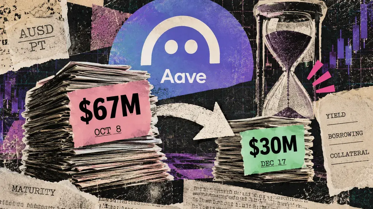
Aave and Pendle may have found a way to keep yield capital f...
31 minutes ago
0

Ripple News: Why $1.53 Matters for the Token’s Next Move
40 minutes ago
0

Best altcoins to buy in October 2026: Five tokens to track
49 minutes ago
0
AI startups shift to cheaper Chinese models as US firms face...
50 minutes ago
0

Hyperscale Data reports about 220 Bitcoin and $37.4 million ...
58 minutes ago
0
Popular

Starknet shields 45 assets with new privacy framework
4 weeks ago
99






Chainflip loses 736,442 USDT in TRON exploit
3 weeks ago
41

 English (US) ·
 © Clint's Cryto News 2026. All rights are reserved
