 1 hour ago
2
1 hour ago
2
TSMC and Winbond are collaborating on a localized DRAM supply chain using 3D wafer-on-wafer (WoW) stacking technology, a move designed to keep critical memory production close to home while feeding the demand of AI hardware.
What Winbond brings to the table
Winbond supplies specialized DRAM wafers designed for next-generation WoW stacking processes. Its proprietary architecture, called CUBE (Customized Ultra-Bandwidth Elements), is purpose-built for this kind of integration. CUBE offers scalable memory options with densities ranging from 256Mb to 8Gb per die. TSMC handles the stacking and integration through its existing SoIC/WoW packaging capabilities.
Why localization matters now
TSMC’s Parts Localization Program, initiated in 2024, has contributed over NT$2 billion (roughly $62 million) in annual output value and reduced validation times by approximately 50% as of February 2026. The Winbond DRAM collaboration fits into that broader effort.
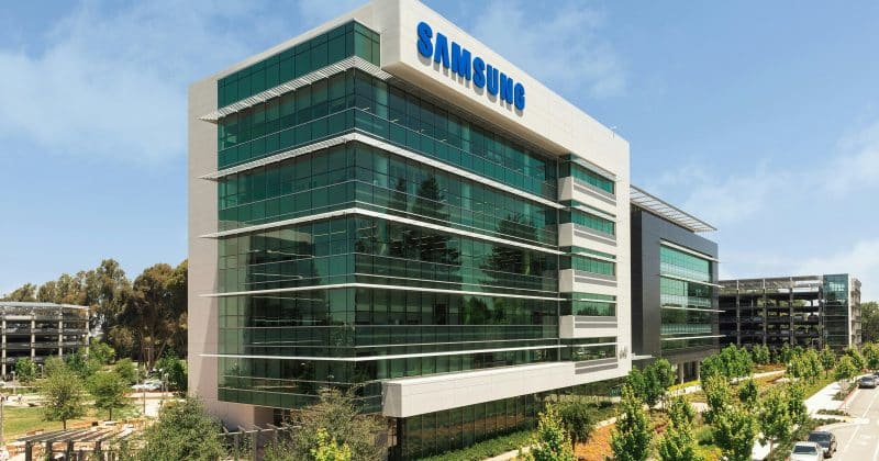
Most high-bandwidth memory (HBM) used in AI training today comes from Samsung and SK Hynix in South Korea. By developing an alternative DRAM integration pathway within Taiwan, TSMC reduces its dependency on external memory suppliers for certain applications.
UMC, Taiwan’s second-largest foundry, publicly announced its own wafer-to-wafer 3D IC initiative involving Winbond and other partners on October 31, 2023.
What this means for investors
Neither company has publicly disclosed yield data or production timelines for this specific collaboration. Specific details surrounding the TSMC-Winbond collaboration remain sparse, as neither company has issued significant announcements regarding the project.
Disclosure: This article was edited by Editorial Team. For more information on how we create and review content, see our Editorial Policy.


 English (US) ·