 2 hours ago
1
2 hours ago
1
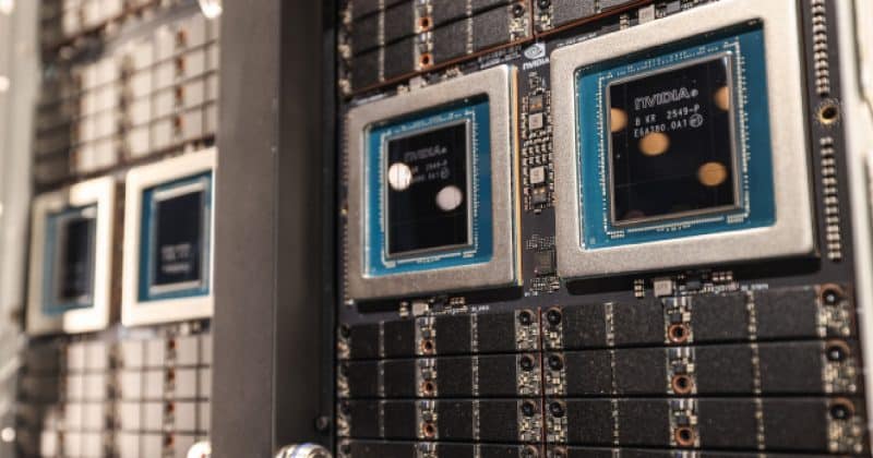
SK Hynix is pouring an almost incomprehensible amount of money into its future. The South Korean semiconductor powerhouse has laid out a total investment plan of KRW 1,100 trillion, roughly $800B, spanning key manufacturing sites including Yongin, Cheongju, and a newly designated southwestern cluster.
At the center of the near-term roadmap sits the M17 front-end fabrication plant in Cheongju. The facility is part of a broader upgrade strategy for what is already one of SK Hynix’s most critical memory production hubs.
What the M17 facility actually means
The M17 project first surfaced back in 2022, when the company floated plans for a new NAND flash fab alongside its existing M11 and M12 facilities in Cheongju. Construction timelines got pushed back due to market turbulence that affected the broader semiconductor industry.
Now the project is back on track. Under a 2026 investment plan, SK Hynix has allocated KRW 100 trillion specifically for follow-on developments at the M17 plant. That allocation also covers an advanced packaging facility referred to as P&T7, which will play a key role in the company’s high-bandwidth memory ambitions.
SK Hynix is targeting mass production of HBM5, its next-generation high-bandwidth memory variant, around 2029 to 2030, aligning these timelines with expected advancements in AI-driven GPU technologies.
The bigger production picture
Chairman Chey Tae-won has outlined goals to double SK Hynix’s wafer production capacity within the next five years from June 2026, and to triple it by 2034.
The southwestern cluster represents a newer geographic bet, diversifying SK Hynix’s manufacturing footprint across South Korea. Combined with the Yongin developments, the company is building out a multi-site production network.
What this means for investors watching the AI hardware race
SK Hynix is one of only three companies globally, alongside Samsung and Micron, that can produce high-bandwidth memory at scale. The HBM5 mass production timeline of 2029 to 2030 aligns with industry expectations for the next generation of AI accelerators.
That said, SK Hynix itself has no apparent connection to cryptocurrency tokens or blockchain initiatives. This is a pure-play semiconductor investment story focused on memory technology.
The risk, as always with massive capital expenditure programs, is that demand projections don’t materialize at the expected pace. The semiconductor industry has a long history of boom-bust cycles driven by optimistic overbuilding.
Disclosure: This article was edited by Editorial Team. For more information on how we create and review content, see our Editorial Policy.


 English (US) ·